


News & Events
Just weeks after demonstrating its ability to make 300-mm CMOS wafers using a thin layer of diamond, EE Times caught up with Akhan Semiconductor Chairman Adam Khan for a follow-up to our previous interview on the company’s prospects.
Diamond is likely to replace some special materials such as silicon carbide and gallium nitride in semiconductor applications for military and aerospace, according to Khan. Operation in high-temperature, high-power environments is a basic requirement for new materials that extend the performance of silicon, he said. Khan also sees new applications for diamond CMOS in the much larger automotive sector, with its own demands for operation in hot, high-power applications.
“Everything that you’ve seen in silicon carbide and gallium nitride markets can easily be a segment of diamond,” Khan said in the interview. “Those materials are not so entrenched at this point that they would be massively disruptive to the market.”
Diamond is a direct competitor to silicon carbide, he asserted. Instead of the 200°C (392°F) upper limit of silicon carbide, diamond can operate above 500°C without degradation, he noted.
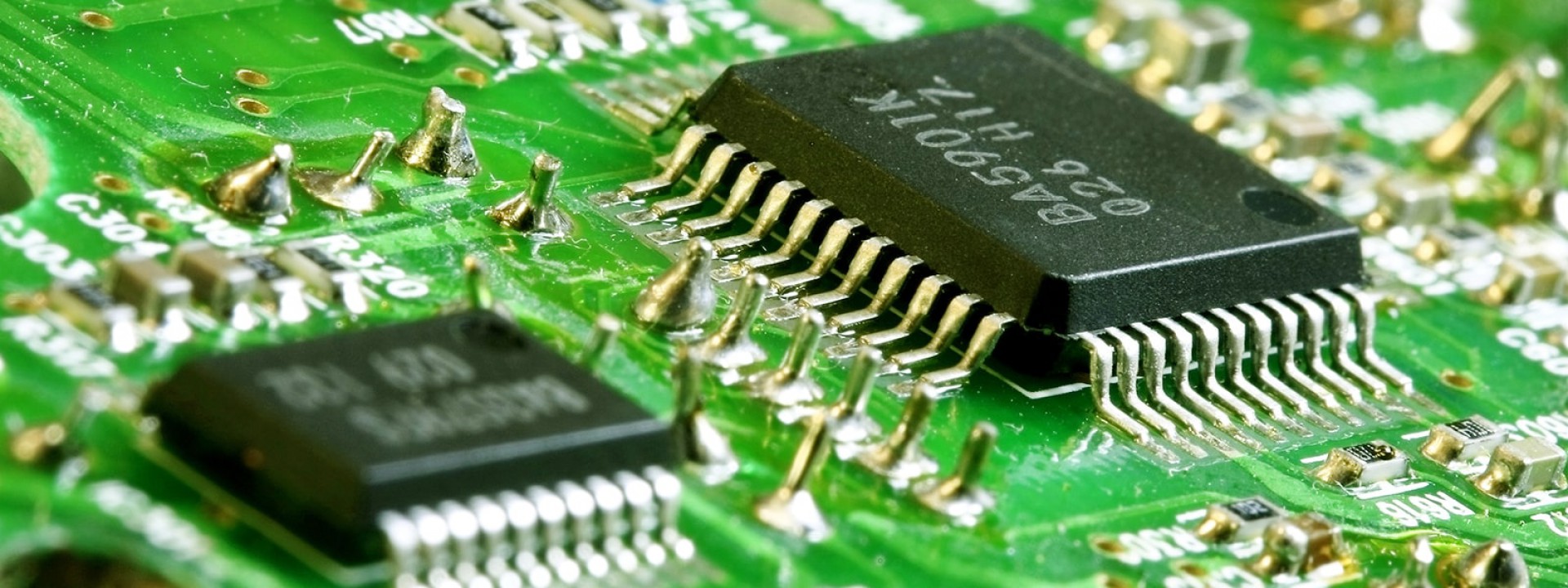
The company has been making 200-mm diamond wafers since 2014 for customers such as Lockheed Martin and Honeywell. Akhan’s shift to 300-mm wafers was as necessary step to meet demand for a wider range of devices.
Many of the same challenges faced in mil-aero applications such as high temperatures apply to the automotive sector, where the overall thermal budget for engines must be reduced. Akhan is betting its shift to 300 mm will make diamond compatible with existing processes and fab lines while lowering per-unit cost to a point that is competitive—even with silicon—as soon as 2024, according to Khan.
“Since we’re doing a very thin layer of diamond, we’ve previously used a metric that is per-unit area or pound-for-pound cheaper than gallium nitride. It’s now cheaper than silicon carbide as well.
“The only material that it is not cheaper is silicon,” Khan added. “The economies of scale are so massive that, of course, diamond is still more costly than silicon. With adoption, we want to approach those price points, that diamond should be cheaper than silicon, not only in terms of performance per unit area, but also performance savings.
“We’ll be doing less mask layers. We’ll have less dense circuitry, which will accomplish greater functionality for the cost. The system cost should actually come into parity with silicon,” he argued.
Non-seismic shift
Still, diamond will not represent a “seismic shift” away from silicon, Khan acknowledged.
One major factor hindering diamond adoption is the semiconductor doping process. P-type, or boron doping, of diamond has yielded some additional conductivity, but nowhere near the achievements of silicon carbide.
N-type doping of diamond using arsenic or phosphorus, a focus of research since the 1960s, has been Akhan’s target for commercialization.
“We can now start to go after RF and power RF applications,” Khan said. The value is evident in silicon carbide, where it can operate at higher temperatures and higher power density than silicon. Diamond is far superior,” Khan claimed.
The company’s 300-mm wafer capability demonstrates that aside from the special diamond tools, other fab tools for lithography or metallization are the same as those already used in fabs.
While Akhan aims for cost parity, comparisons between silicon and diamond are not trivial for a variety of applications. Key factors include the level of doping and the number of mask levels. Diamond’s advantages include the elimination of thermal and material layers and adoption of simpler packaging.
“That’s what we’ll be doing in the coming months as we demonstrate some of these devices,” said Khan.
For now, diamond remains a niche material in that it’s significantly tied into the aerospace and military segments.
“You’re going to see a massive uptake in this, because with automotive, then comes industrial and some other use cases. Then we’re going to see a lot more adoption and I would say a lot more competition from some of the other diamond players in the world.”
R&D still resides mostly in universities such as the Massachusetts Institute of Technology and Stanford. That will contribute to the rise of new diamond market competitors, according to Khan.
Akhan expects to announce new partnerships soon with some of its existing customers. As with the startups above, Khan declined to name the partners.
“We have major customers that are pulling the technology. This really hasn’t been seen before. There haven’t been these major customers that are now directing the fabs. We’ve adopted diamond processes, and now we’re directing the fabs to utilize these processes and materials. And that’s been really the major difference maker, particularly in the last 12 months or so.”
“Customers have crossed the scale part of the equation, so that we’re able to now address specific problems, whether it be hardness, thermal or power density,” Khan said. “We work with the customers and do the proof of concept, the low-volume pilot production and then transfer technology to the fabs that actually have volume production.”
Soon, he predicted, “this will be for things like power inverters for automotive applications. I think that’s where it gets quite exciting.”
By DIGITIMES
