


News & Events
California startup Ayar Labs is building an ecosystem around its optical chip–to–chip communication technology. The company has partnered with Nvidia to develop next–generation architectures with optical I/O.
“Over the past decade, Nvidia–accelerated computing has delivered a million–X speedup in AI,” said Rob Ober, chief platform architect for data center products at Nvidia, in a statement. “The next million–X will require new, advanced technologies like optical I/O to support the bandwidth, power, and scale requirements of future AI and ML workloads and system architectures.”
“We’ve been engaging with Nvidia behind the scenes for a while,” Ayar Labs’ president and CTO, Mark Wade, told EE Times. “They’re looking to get something like an order of magnitude of system–level performance increase per year, and what they’re finding is that the fabric performance is severely limiting and bottlenecking them now.”
“We’ve been well–aligned to Nvidia’s problem statement for a long time,” Wade said. “If you want to build massive scale–out systems that can go far beyond what they’re able to do right now… if you want to get to many thousands of GPUs that are logically connected, all crunching on the same neural net problem, then you have to solve the scale–out fabric problem. And I think we’re aligned with [Nvidia] on the solution direction, which is that from the first principles of physics, photonics and optics are the only way to do it.”
Nvidia’s official line is that it believes AI models will have 100 trillion or more connections by 2023 (600x more than in 2021), and that at this point, the technical capabilities of existing copper interconnect platforms will have been exceeded. Ayar claims its optical chip–to–chip communication technologies can provide 1000x the bandwidth density of copper interconnects at one–tenth of the power and latency.
OPTICAL FIBER
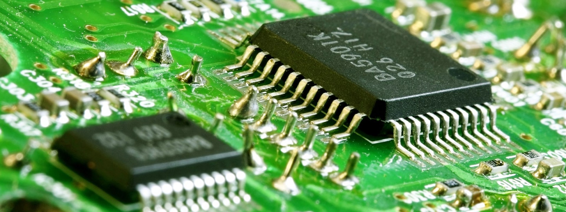
Ayar has been working on optical I/O technology since it spun out of MIT, University of Colorado Boulder, and University of California, Berkeley in 2015. The company’s TeraPHY chiplets sit alongside a host SoC to enable high bandwidth, high speed, low power optical chip–to–chip communication via optical fiber.
“Generation after generation, we’re still scaling compute per reticle,” Wade said. “But at the same time, I/O bandwidths were very much struggling to keep pace, even in the 2010s… How will electrical I/O technologies fare in attempting to escape that bandwidth limit?”
This problem manifests itself in a number of dimensions, including the amount of power required for I/O and the amount of bandwidth required per computational unit. Electrical links are starting to require re–timers, with a corresponding increase in system level cost and complexity.
Ayar’s technology is built to address these issues. The company fabricates its optical I/O chiplets at GlobalFoundries and ships known good die to customers, where they are flip–chip assembled next to a host SoC on a module, enabled by modern chiplet interposer technology. Ayar’s TeraPHY chiplets take care of electrical to optical conversion, so that data can travel between chips using optical fibers.
Today, Ayar uses an electrical interface between host SoC and optical chiplet that it designed with Intel in 2018 as part of the DARPA PIPES project (see below). However, the company plans to be compatible with both UCIe and CXL chiplet–to–chiplet communication standards going forwards.
“We’re really excited about [the UCIe] spec,” Wade said. “We think it’s going to be a strong driving force to converge solutions… all chiplet providers face this issue. You don’t want to fragment your product roadmap into a million different SKUs. UCIe is going to drive some alignment here, and we’re excited about that.”
One of Ayar’s key decisions early on was to separate the light source itself from the photonics chiplets (Ayar Labs has its own standalone multi–wavelength laser light source called SuperNova).
“The physics of lasers are disconnected from the physics of CMOS microelectronics; they don’t like to operate at high temperatures,” Wade said. “They rapidly lose power efficiency and their reliability gets exponentially worse.”
High TDP compute nodes use hundreds of Watts; the temperature inside an SoC package might be 80°C or above. Disaggregating the light source from the SoC allows it to be placed further away, keeping its temperature below 55°C.
BUILDING AN ECOSYSTEM
Intel selected Ayar Labs to provide the optical I/O for its DARPA PIPES (photonics in the package for extreme scalability) project in 2019. The project demonstrated Ayar’s chiplets working alongside an Intel FPGA die, but Ayar’s partnership with Intel now branches beyond FPGAs, Wade explained.
“The question was, is Ayar’s interesting technology going to be able to be designed, manufactured, and assembled less than a millimeter away from a precious full–reticle SoC in a way that actually solves the SoC’s problems?” Wade said. “Working on [the DARPA PIPES project] was really proving out our technology and product architecture… it was a major proof point.”
Intel Capital is now a strategic investor in Ayar Labs.
Hewlett Packard Enterprise is another strategic investor in the company (via its VC arm, Hewlett Packard Pathfinder), coming in alongside Nvidia during Ayar’s $130-million series C round in April. Wade points out that the roadmap for HPE’s Slingshot fabric — an HPC fabric originated by system integrator Cray which was acquired by HPE in 2019 — requires optical I/O chiplets going forward.
“Platforms are going to become more heterogeneous, moving around a lot more bandwidth between different kinds of sockets,” Wade said. “HPE is on the forefront, trying to figure out what fabric solutions can actually make this heterogeneous vision performant.”
HPE and Ayar will collaborate on photonics R&D to build a joint ecosystem of solutions and customers.
Another strategic investor, Lockheed Martin, has a number of interesting needs in the defense segment, but the breakdown of electrical I/O is ubiquitous, according to Wade.
“The collision course of I/O power and TDP is happening right now, and over the next decade or so, we’ll see a photonics transformation across all segments and verticals,” he said.
Other strategic investors include GlobalFoundries and Applied Ventures (the VC arm of Applied Materials).
TIMING IT RIGHT
Why is this the right time for optical I/O to emerge — is the technology finally ready, or is the market demand finally there?
“The key technology aspects have been de–risked since about 2018,” Wade said. “The main driver that needed to happen was that the end market demand would be strong enough to align the high–volume, advanced manufacturing supply chain to make it happen.”
Wade compared bringing advanced technologies to market to a chicken–and–egg problem; de–risking the technology helps create market demand, which helped align some key high volume manufacturers in the critical path along the supply chain, he said.
“My opinion is that we’re going to be rate–limited by establishing the supply chain,” he said. “We’re [production] qualifying the technology this year, which drives the majority of our engineering focus. At the same time, we’re doing a lot of work to make sure we’ve got the end–to–end supply chain ready to hit that ramp that we’re targeting a couple of years into the future.”
Ayar Labs plans to focus on building scale for its products through partnerships and ecosystem development this year, and expects to ship “thousands of units” by year end.
By EETimes
