


News & Events
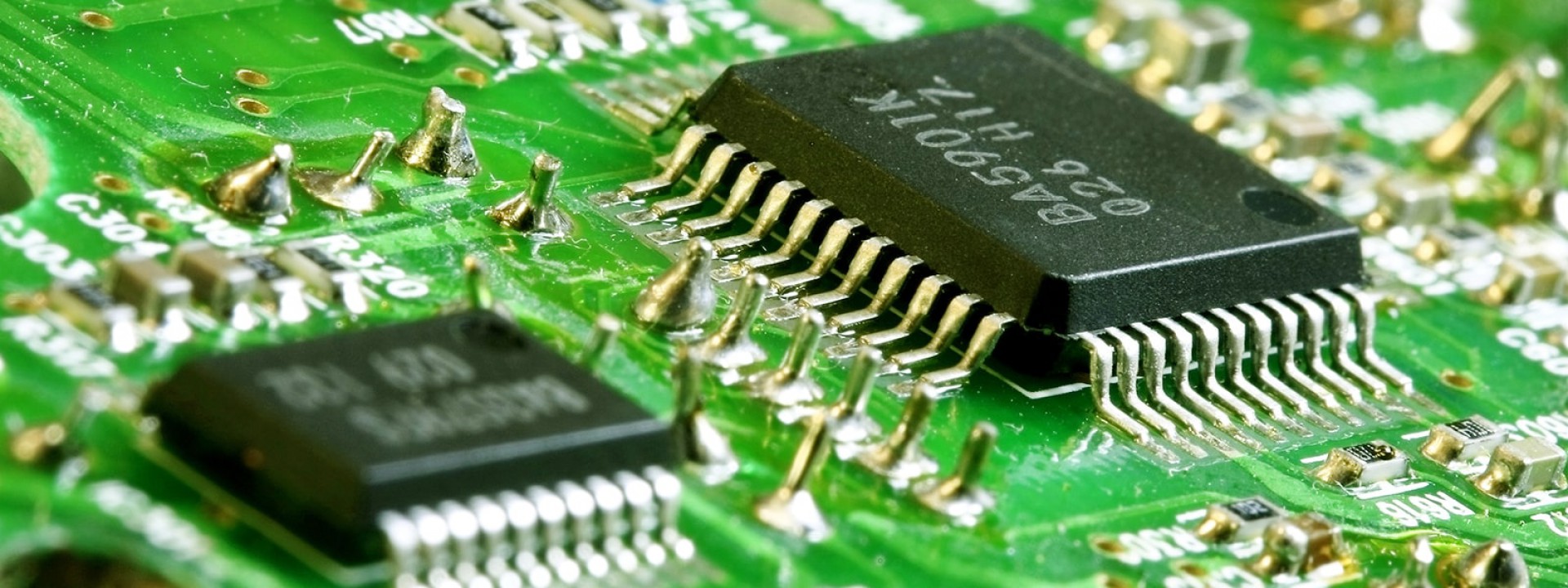
Semiconductor device manufacturing requires the availability of high-quality wafers with perfectly flat and smooth surfaces. The quality of a wafer’s surface is fundamental to ensuring high-performing and reliable devices. It is necessary to prevent the formation of impurities or surface irregularities that could introduce defects in the final component and lead to increased costs.
An innovative device lift-off and substrate reuse technology based on the power of sound, under development at Crystal Sonic, Inc., aims to lower per-device manufacturing costs substantially.
Today, nearly 50% of wide bandgap (WBG) device manufacturing costs are attributed to the substrate material. At the same time, WBG substrate wafer demand is ramping up, mainly driven by applications including automotive, solar inverters, motor, and wind inverters, particularly for silicon carbide (SiC).
The gap between demand and availability of wafers is expected to widen in the coming years, with the potential risk for SiC wafer shortages. The demand for gallium nitride (GaN) is also growing rapidly, driven by the radio frequency (RF) and automotive sectors, as well as by all applications that require high power density, high efficiency, high switching frequency and small dimensions.
A promising way to close this gap is through substrate reuse technologies.
Crystal Sonic’s substrate reuse tech
Headquartered in Phoenix, Arizona, Crystal Sonic is a hard-tech startup founded in 2018 with the goal of reducing costs and material waste to produce next-gen semiconductors.
Crystal Sonic’s device lift-off and substrate reuse tech, which holds two awarded and active patents in the U.S. and Japan (plus another patent pending and three additional patent filings in preparation), originates from Professor Mariana Bertoni’s laboratory at Arizona State University (ASU). Bertoni leads the Defect Engineering for Energy Conversion Technologies (DEfECT) lab, focusing on how defects can affect a material’s electrical and optical properties.
The patented process, known as Sonic Lift-Off, uses sound waves to cut single crystal wafers used in semiconductor-based device fabrication, preventing waste, and saving money. Unlike the traditional grinding process, which is expensive, time consuming and introduces damage to surfaces and sub-surfaces, Crystal Sonic’s tech uses sound to cut and lift-off thin device layers, leaving high quality surfaces behind and the bulk substrate available for reuse.
By replacing mechanical wafer backgrinding with reuse tech, allowing manufacturers to reduce the device’s wafer cost contribution (approximately 50% of total cost) by half and potentially towards zero with multiple reuses.
According to Crystal Sonic, next-gen semiconductor devices are being built on substrate materials like SiC, GaN, gallium arsenide (GaAs) and others. These materials produce smaller, more effective and more efficient devices, opening new possibilities for power electronics, sensing, communications and other fields.
Due to their reliability, efficiency and performance, WBG materials are rapidly growing in the market, meeting demand from megatrends like e-mobility, photovoltaics, laser diode, radio frequency and healthcare/disinfection.
Sonic Lift-Off
Device thinning is a crucial step in the manufacturing processes at the back end. The traditional (established) method is mechanical backgrinding, but it is inefficient, time-consuming and expensive to use (as mentioned before, 50% of the overall device manufacturing cost is attributed to the wafer).
As shown in Figure 1, Step 2 of the conventional manufacturing workflow consists in the device fabrication, while Step 3 is the backgrinding (device thinning), followed by the dicing and packaging steps. During backgrinding, legacy manufacturing techniques for wafering and device thinning waste 90% or more of the substrate material, which cannot be reused.
Crystal Sonic’s patented solution, Sonic Lift-Off, harnesses the power of sound to separate thin devices from semiconductor substrates, enabling substrate reuse. Described as a superior substitute for inefficient mechanical grinding and polishing, Sonic Lift-Off uses sonic energy to cut substrates without leaving any material behind.
As shown in Figure 2, this alternative to backgrinding is fast, wastes no material, and maintains high quality surfaces with micron precision. By reusing the substrate, the largest contribution to the overall manufacturing cost can be drastically reduced.
To date, Crystal Sonice has successful performed demos and prototype testing on small diameter Si, GaAs, SiC, GaN and AlN wafers. The tests performed produced satisfactory results in terms of thickness control, low-roughness surfaces, and preserved device performance. Moreover—which is even more relevant and depicted in Figure 3—the performance of the device built with reused substrate is practically the same as with the original substrate.
Traditional wafer backgrinding reduces the wafer thickness using a diamond-resin bonded grinding wheel to remove the semiconductor material from the back of a wafer. This is a legacy and established technique, but it is costly, wasteful and reuse of material is not possible. Moreover, it requires deionized water to wash debris from the surface and prevent contamination.
Besides backgrinding, other device thinning methods are currently available, such as the chemical (ELO), mechanical (spalling), laser Lift-Off, smart cut (ion implantation), and 2DLT (remote epitaxy) techniques. Though Sonic Lift-Off is still under development, the solution (also known as acoustic spalling) is the only one able to provide the following characteristics:
- Tunable lift-off thickness,
- Fast, scalable process,
- High-quality surfaces,
- Multiple reuses and
- Multiple substrate types.
Regarding the sub-surface damage, Sonic Lift-Off provides low roughness (Ra < 1 µm, to date), minimal or no sub-surface damage, can maintain off-cut angle (due to acoustic control), is a gentler and material-efficient process, and allows reuse of multiple substrates.
“Reusability allows device manufacturers to reclaim the most expensive part of the device manufacturing process, which in turn drives down the cost of next generation semiconductor devices,” according to Crystal Sonic.
By EETimes
