


News & Events
t Hot Chips this week, Untether unveiled its second-gen architecture for AI inference, the first chip using this architecture, as well as plans to expand to edge and endpoint accelerators.
Untether’s new architecture, internally codenamed Boqueria, addresses trends for very large neural networks, including transformer networks in natural language processing and beyond, endpoint applications that require power efficiency, and applications that require performance and power efficiency combined with prediction accuracy.
The first chip to use the Boqueria architecture, SpeedAI, is a data center inference accelerator capable of 2 PFLOPS of FP8 performance running at peak power consumption (66 W), or 30 TFLOPS/W based on a more usual 30-35 W power envelope. (Untether’s first generation chip, RunAI, could handle 500 TOPS of INT8.)
This level of performance translates to running BERT-base inference at 750 queries per second per Watt, which the company says is 15× the performance of a state-of-the-art GPU.
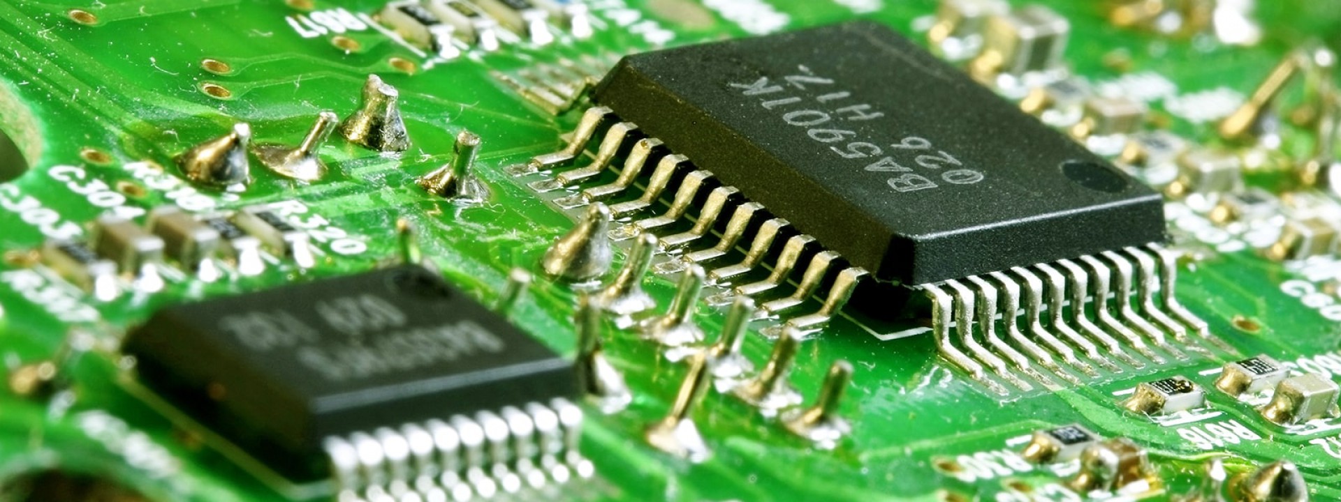
The 35 by 35-mm chip is built on TSMC’s 7 nm technology and uses more than 1,400 optimized RISC-V cores—the most EE Times has seen in a commercial chip (beating the previous record holder, Esperanto).
“[The performance] is a convergence of different factors,” Bob Beachler, VP of product at Untether, told EE Times. “It’s a combination of a lot of things, including circuit design, data types, understanding how neural networks operate—how does a transformer operate compared to a convolutional network?—all of these things we’ve been able to embody in our second-generation chip.”
Untether carefully considered the balance between flexibility, performance, and scalability when working on Boqueria.
“To make general-purpose AI compute architecture, you have to have the right level of granularity and flexibility to efficiently be able to run this plethora of neural networks and be able to scale from small to large,” Beachler said. Accuracy is also important for inference workloads, he added, particularly for recommendation where any percentage points of accuracy loss can mean substantial financial losses, and for safety-oriented applications like autonomous driving.
AT-MEMORY COMPUTE
Untether’s second-gen architecture, Boqueria, is based on the same at-memory compute concept as the first gen. The chip has a total of 238 MB of SRAM arranged into 729 memory banks with around 1 PB/s memory bandwidth total. The memory banks contain processing elements, controller cores, and networking elements.
Each memory bank has two RISC-V processors, replacing the homegrown RISC design in the first gen. These are multi-thread capable, driving multiple rows of processing elements at the same time, which adds to granularity and efficiency. Untether has added more than 20 custom instructions for tasks, including matrix vector multiplication and row reduce functions, such as SoftMax or LayerNorm, found in transformer networks.
Beachler explained that in the first gen, the processing elements in each memory bank were controlled by a single controller that would execute the same instruction (or not execute it). In Boqueria, this is now controlled on a per-row basis, so that each of the 8 rows of the 64 processing elements can operate independently. This reduction in granularity increases efficiency, since different instructions can be processed within the same memory bank.
Processing elements retain their zero-detect circuitry, which saves power in sparse networks. There is hardware support for 2:1 structured sparsity, as well.
SRAM in the memory banks is the standard 6-transistor cell, with voltage of the data path reduced to 0.4 V to save energy thanks to migration from TSMC’s 16 nm to 7 nm.
The “rotator cuff” interconnect, which rotates activations between processing elements to save energy, remains. There is a new packet-based network on chip, which transports packets East-West and North-South within and between memory banks.
FLOATING POINT SUPPORT
Untether’s processing elements support INT4, INT8, and BF16, as well as Untether’s own FP8 formats. The company has decided on two FP8 formats designed to balance energy efficiency, throughput, and prediction accuracy. The two formats have a 4-bit mantissa (what Untether calls FP8p, for precision) or a 3-bit mantissa (Untether’s FP8r, for range). (Note that these are 1-mantissa-bit more precise than Nvidia’s FP8p and FP8r formats used in training).
According to Untether, this implementation of FP8 represents a sweet spot that results in less than 0.1 percentage points of accuracy loss compared to BF16, but is four times more energy efficient. This is achieved purely by quantization (no retraining required).
SCALABILITY FEATURES
New scalability features include two LPDDR ports for up to 32 GB of external memory. This would allow coefficient and layer swapping in single-chip systems where a network being computed was larger than the chip could hold.
There are also three PCIe Gen5 chip-to-chip interfaces for host-to-accelerator and accelerator-to-accelerator communications.
SpeedAI chips will be available on M.2 modules, or 12-PFLOP 6-chip PCIe cards. Untether’s software development kit (SDK), updated for the new hardware, can handle quantization to Untether’s FP8 formats, optimization, physical allocation, and partitioning of large networks across multiple chips or cards in a cluster.
CHIPLET FRIENDLY
Untether also hinted at plans to make smaller chips based on the same Boqueria architecture, targeting a variety of different classes of edge and endpoint systems. The company is planning a 25-Watt chip for infrastructure, a 5-Watt chip for perception in autonomous vehicles, and a sub-1-Watt chip for battery operated devices (the specific example given was law enforcement or military body cameras).
This is in part enabled by the ability to use external memory if required, so that sections of networks can be processed sequentially as they are brought in from DRAM. There is a latency hit, but it means smaller chips can run larger networks.
Beachler also points out that Boqueria-based chips are “chiplet friendly.”
“Because we have the I/O NOC and peripherals, we could easily swap out the PCI Express and put in a UCI Express for die-to-die communication,” he said. “We fully anticipate at some point in the next five years we’ll have customers wanting to do die-to-die interconnect and wanting to use some kind of die-to-die IP.”
Founded in Toronto in 2018, Untether is funded by CPPIB, General Motors, Intel Capital, Radical Ventures, and Tracker Capital. The startup has raised just over $170 million and has close to 200 employees and contractors.
The company only recently revealed that General Motors was one of its investors. The two companies have been working together on a project part-funded by the Ontario government concerning autonomous vehicle perception systems. This work will form the basis of a future line of automotive-grade parts, Beachler said.
SpeedAI chips on M.2 modules and PCIe cards will be sampling to early access customers in the first half of 2023.
By EETimes
